MRAM Test
What is MRAM?
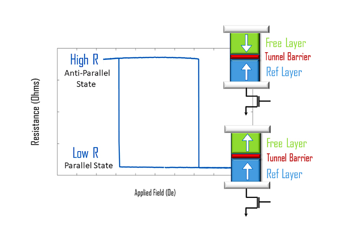
Unlike conventional semiconductor memories that store data as electrical charges, MRAM (Magnetoresistive Random Access Memory) is a non-volatile memory in which data bits are stored using the magnetization (e.g. electrons spin) orientation.
MRAM offers a number of advantages compared to existing semiconductor technologies, as it is intrinsically nonvolatile (e.g. capable of holding data when the power is cut off), whilst also exhibiting very good endurance (e.g. number of read/write cycles) and low operating power. The last generation of MRAM called pSTT-MRAM (Perpendicular Spin Transfer Torque Random Access Memory) has been chosen by the industry to replace embedded Flash at technology nodes below 28/22nm and is now readily available at major semiconductor foundries.
How did MRAM devices evolve?
The first generation of MRAM was based upon the so-called toggle technology, in which the data is written (e.g. the magnetization is flipped) by an internal magnetic field. Toggle MRAM has been and still is very successful, but it is power-hungry and difficult to scale down. Succeeding generations of MRAM devices started to use another method called Spin Torque Transfer (STT) MRAM. STT-MRAM uses a spin-polarized current to write data. This approach has the advantage of providing lower and scalable switching currents resulting in higher density memory products.
What are the applications of MRAM?
Industry interest in pSTT-MRAM as the embedded nonvolatile memory (eNVM) of choice for advanced technology nodes has been confirmed by the production schedules of Tier 1 semiconductor foundries. STT MRAM is now ready for volume production in applications as diverse as industrial, automotive, IoT, mobile, AI and ultimately computing and storage.
What is the future of MRAM?
Whilst STT MRAM is currently being deployed as a mainstream NVM technology, researchers around the globe are already looking at the next generation, called SOT-MRAM (Spin Orbit torque MRAM). By enabling simultaneously infinite endurance and high speed, which STT cannot, SOT can broaden the use of MRAM to cache memory. SOT-MRAM has the potential to become a universal embedded memory, replacing simultaneously embedded NVM and/or embedded SRAM in microcontrollers, microprocessors and System-on-Chips.
What are the MRAM Market projections?
According to a report from Objective Analysis and Coughlin Associates dated May 2020, the market for emerging memories will hit $36B by 2030. This spectacular raise will largely be fueled by displacing current technologies such as embedded NOR flash and SRAM blocks in microcontrollers, processors and ASICs, as well as specialty standalone DRAM memory chips.
Additionally, industry’s migration to emerging memory technologies will launch a solid increase in capital equipment spending, with a corresponding manufacturing equipment revenue of $696M.
What is Hprobe’s contribution to the success of MRAM?
The availability of high throughput, highly reliable back end of line (BEOL) manufacturing equipment is key to the onset of new semiconductor technologies. As an automatic test equipment (ATE) provider with a unique expertise in MRAM, Hprobe offers IC manufacturers with a turn-key solution that will accelerate MRAM product development, ensuring a successful ramp-up.
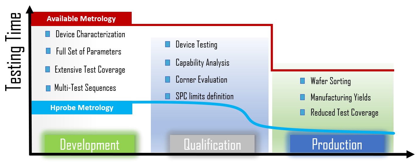
Testing time is the key performance indicator in production and a strong added value to reduce development time. Building the optimal wafer test equipment dedicated to STT-MRAM technology with the maximum flexibility and shortest testing time brings strong value during the development phase and reduces the ramp-up time to high-volume manufacturing (HVM). Hprobe solutions fulfill the conflicting needs for flexibility and performance, therein supporting engineers on their long road from technology release to production control and monitoring.
How do Hprobe products operate?
By nature, MRAM requires wafers to be electrically tested whilst applying an external magnetic field. In addition, the probing must be done with high-frequency hardware that provides the ultra-narrow time domain voltage/current pulses at which MRAM devices operate.
As such, the wafer-level parametric testing is done by:
Sweeping a magnetic field (perpendicular and/or planar) above the device whilst sensing the device resistance by a DC current. This allows to extract the hysteresis curve, which reflects the ability of the memory cell to switch from one state to another and to retain the stored information. The perpendicular magnetic field must be as high as 5000 Oersted (0.5 Tesla) to switch both the various magnetic layers in the device.
Applying a pulsed signal with an ultra-narrow pulse width (down to 300ps and up to 5V amplitude) to the device to duplicate the on-chip read/write operation, as well as to characterize its reliability (breakdown voltage).
Once the wafers manufacturing is finished and the chips are completed, testing needs to be performed under external magnetic field to characterize the strength of the MRAM block to operate under environment-related disturbing magnetic fields.
This can be done either at the wafer level, prior to dicing, or at the packaged chip level. In both cases, one needs the ability to apply 3-dimensional magnetic fields onto an Automated Test Equipment.


